Poster presented at NSS2000 Conference, Lyon France, 15 - 20 October 2000
Driving Energy Resolution to the Noise Limit
in Semiconductor Gamma Detector Arrays
Uri Lachish
guma science, P.O. Box 2104, Rehovot 76120, Israel
![]()
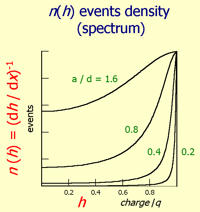
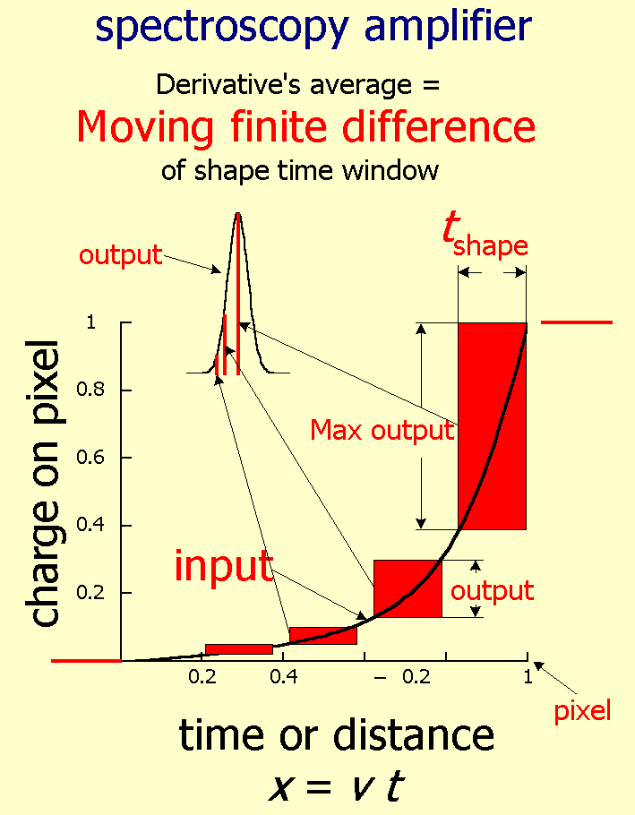
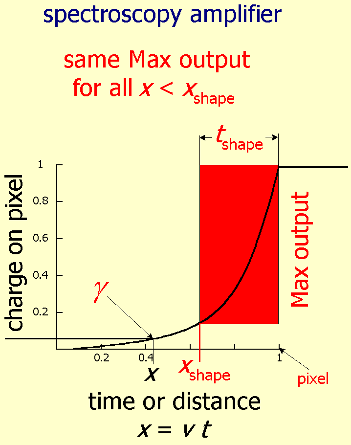
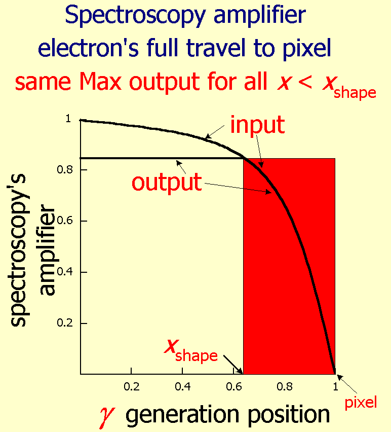
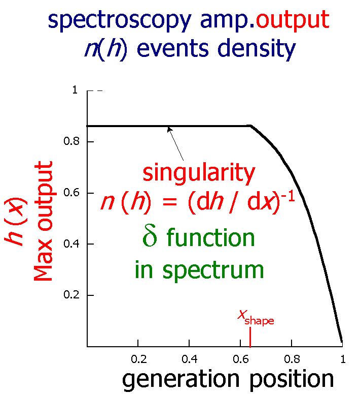
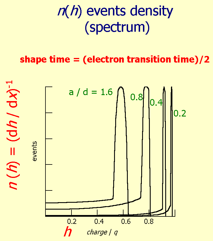
Shape time adjustment below the electron transition time from contact to contact enhances resolution
Published Data:
Resolution higher than theory
|
Ref. |
Source (kev) (1) |
a /d(2) |
Line width (%) (3) |
|
|
Measured |
Calculated |
|||
|
[1] |
22 Na (511) |
0.3 |
2.13 |
2.7 |
|
[2] |
133 Ba(356) |
0.38 |
2.6 |
4.2 |
|
[3] |
137 Cs(662) |
0.38 |
1.7 |
4.2 |
(1). Gamma sources of nearly uniform excitation.
(2). a/d: ratio of pixel size to thickness.
(3). Calculation by small pixel theory.
Consequence:
Gamma energy resolution of a single pixel, of a detector array *, improves dramatically by shape time optimization.
* Including single detector with a guard ring surrounding the positive contact.