(see https://urila.tripod.com/crystal.htm)
Abstract: Gamma induced photo-currents in semiconductor
radiation detectors, equipped with ohmic contacts, are not sensitive
to low hole mobility, or hole trapping. The device design is discussed
and experimental results are presented.
PACs: 07.85-m, 72.40.+w, 72.80.Ey, 73.40.Kp.
Keywords: gamma, radiation, detectors, ohmic, blocking, contacts
"experientia docet"
The amount of charge photogenerated by a gamma photon in a semiconductor detector is proportional to its energy. Therefore, this energy is measurable by full charge collection [1]. However, a common problem observed with many semiconductors is that the photogenerated holes tend to be trapped in deep levels within the forbidden band. Therefore, partial charge collection leads to signal dispersion and low resolution in measurements of gamma energy.
Efforts have been made to overcome the hole trapping problem, either by electronic signal processing, where an external circuit compensates charge trapping [2 - 6], or by design of detectors of various geometrical shapes, and recently, by application of grid structure contacts [7 - 10]. However, these methods seem suitable to improve single detector devices, but they are rather complicate or are not practical for multi-element detector arrays.
A recent article discusses semiconductor detectors equipped with ohmic contacts [11]. It proposes that the flow of the gamma photo-generated charge, towards the contacts, is accompanied by additional charge flow from the contacts towards the photo-generated charge. Thus, electrons, that enter the bulk from the negative contact, flow towards the holes and recombine with them. A calculation of a model detector indicates that this flow more than compensates for the hole low mobility or hole trapping. Therefore, ohmic contact detectors are not sensitive to the slow or even lack of hole movement, and there is no need of trapping compensation by an external circuit.
Optimal gamma detector operation is achieved with a device that has the lowest leakage current and the highest mt (mobility times lifetime) values. Since the electron mobility is usually higher than the hole mobility, the material of highest electrical resistance will be p-type.
The charge carriers lifetimes depend on the traps density and distribution within the forbidden band. Trap levels that lie above the Fermi level act as electron traps and levels below it act as hole traps. If there are many levels at mid gap, then shift of the Fermi level, upward or downward, will increase the lifetime of one charge carrier on expense of the other carrier. Since ohmic contact detectors are not sensitive to hole movement, it would be advantageous to increase the electrons lifetime on expense of that of the holes. That is, to shift the conduction towards n-type.
The conduction type is also practically important to fabrication of ohmic contacts. In p-type material the leakage current is that of holes and the photo-current is that of electrons. So, the contacts have to allow the free flow of both carrier types.
In n-type material the contacts need to allow only free electron flow since both the leakage current and photo-current are of electrons. For this reason, if observation of the leakage current indicates that the contacts are ohmic, then the detector will show the ohmic effect of gamma detection.
These arguments indicate that control of the material type and its electrical resistivity is important to achievement of optimal detector performance.
Figure-1 shows the spectra of 57Cobalt and 137Cesium
observed with a CdTe detector equipped with ohmic contacts and
irradiated via the negative contact. CdZnTe detectors show similar
results. The detector is made with n-type material of electrical
resistivity 5 x 10⁸ ohm cm, and its size is 1.5
x 1.5 x 3 mm3
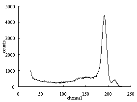
Figure-1: Spectra of 57Cobalt and 137Cesium observed with n-type CdTe detector equipped with ohmic contacts. The FWHM of the 122 kev line of 57Co is 7%, and that of the 662 kev line of 137Cs is 2.2%.
Figure-2 shows the measurement scheme.
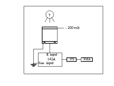
Figure-2: The measurement scheme.
The spectra were taken with Ortec 142A preamplifier, 572 spectroscopy amplifier with a shape time of 0.5 x 10⁻⁶ seconds, and 916A multi channel analyzer (MCA). A bias voltage of V = -200 volts was applied to the negative contact. The positive contact was connected to the preamplifier input, and the bias input was grounded [1]. The positive contact is surrounded with a grounded guard ring, in order to remove the effect of the side walls.
The FWHM of the 122 kev line of 57Cobalt is 7%,
and that of the 662 kev line of 137Cesium is 2.2%.
The electron transition time, tr, through the
detector thickness, d = 3 mm, is:
tr = d2/mV = 0.45 x 10⁻⁶
seconds (1)
where m = 1000 cm2(volt sec)-1 is the electron mobility.
The instrumental shape time is long enough to collect the electrons, but the holes hardly move at all during this period. Therefore, only a partial charge collection and poor energy resolution would have been expected, had there not been other charge flow mechanism. However, the very good resolution observed, mainly with 137Cesium, where charge generation spreads throughout the volume of the detector, indicates nearly full charge collection. The additional flow of electrons, from the negative contact towards the holes, readily explains these results. If the holes do not come to the electrons, the electrons come to the holes.
N-type devices operate well as a result of a combination of two reasons. One is the ohmic contact effect, and one is proper positioning of the Fermi level within the forbidden band, that is, optimal electrical resistivity.
Zanio et al. [12] have published promising results with indium doped detectors that seem to be n-type. However, this work was not continued and then came the THM and HPB p-type detectors. In these detectors the contacts seem, at least partly, to block the entrance of electrons from the negative contact into the bulk. Therefore, the ohmic contact effect is not noticed with them.
The present work points out the potential of n-type material,
that is not sensitive to hole trapping, for efficient gamma detection.
Front detector arrays may combine with back processing arrays
of either crystalline or amorphous silicon. Such devices may prove
useful for conventional detection and single photon detection
of X-rays, especially at higher photon energies.
References:
On the net: 9th, February, 1998
by the author:
Links: