New:
Improving CdTe and CdZnTe Crystals by Agitation during the Crystal Growth
New
Blue Marble the Uniform Earth Image
The Sun and the Moon a Riddle in the Sky
1. Introduction
The application of heavy atom semiconductor detectors to x-ray digital
imaging is discussed with regard to their operation as gamma detectors and
imaging arrays. Section-2 presents a brief overview of x-ray imaging with
amorphous silicon flat panels. Section-3 describes x-ray vs. gamma imaging,
regarding the detector's role in the operation of each system. Section-4
discusses the semiconductor detector and its potential to x-ray imaging.
2. Digital x-ray imaging with amorphous silicon
X-rays are by far the most important medical imaging diagnostic tool. It has been dominated by film sensors since its invention over a hundred years ago. Digital x-ray cameras based on amorphous silicon panels have been developed in the last decade, and are now on the verge of penetrating the market. The new technology employs large area electronic sensors of x-rays that capture the image and transform it directly into an electronic signal [1 - 3].
Amorphous silicon flat panels are produced by a mature technology developed for computer monitors. Silicon is an excellent sensor of visible light. However, it is a light weight atom and transparent to the x-rays applied to medical diagnosis. It is a poor absorber and is not suitable as a direct x-ray sensor.
Coating amorphous silicon with a highly absorbing scintillating layer activates it to x-ray sensing. Figure-1a shows the operation principle of this system. Each x-ray photon, absorbed within the scintillating layer, generates a sparkle of visible light (a scintillation) that is detected by the silicon sensor. The sensor converts the light into electric signal and transmits it to a computer.
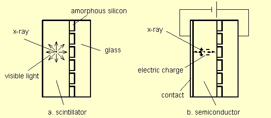
Figure 1: X-ray imaging sensor, a. scintillator, b. semiconductor.
The x-ray generated sparkle of visible light spreads in all directions and reduces the initial x-ray spatial resolution. The resolution improves by reducing the scintillating layer thickness. However, the thinner layer will absorb fewer photons. This imaging x-ray system compromises absorption efficiency and resolution. There is a similar problem with the classical film technology.
Semiconductor detectors largely overcome this limitation by direct conversion of x-rays into electric signals. Figure-1b shows a sensor assembly where a layer of heavy atom semiconductor, covered with a metal contact, replaces the scintillating layer. An x-ray photon, absorbed within the voltage biased semiconductor, generates electric charge that flows towards the contact and the amorphous silicon. The charge flow is perpendicular to the sensor plane, and without spatial spread of signal. The semiconductor layer may be thick enough to absorb all the x-rays without significant loss of resolution.
Semiconductor based imaging sensors are already in advanced state of
development and some systems are on the market. They utilize amorphous selenium
used successfully in photo-copier sensors. However, selenium is not dense and
opaque enough to x-rays, and the electric charge within it is not mobile enough.
Therefore, other materials are considered and tested for this purpose [4 - 6].
It seems, however, that further technology advancement is needed before they
become widespread.
3. X-ray vs. gamma imaging
Figure 2a shows the principle of x-ray imaging. The x-ray photons penetrate
the examined body and generate a projection image of its density distribution on
a detection plane.
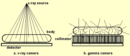
Figure 2: a. x-ray camera, x-ray photons generate a projection image of the
body's density distribution. b. gamma camera, a collimator generates projection
image of radioactive isotope distribution within the body.
In gamma imaging, figure 2b, radioisotopes are infused into the body where they emit gamma photons randomly in all directions. Only small number of the photons that move perpendicular to a planar collimator, cross it and generate a projection image of the radioisotope distribution. The body and the collimator scatter photons that move in other directions. Some of them will cross the collimator at the wrong place and blur the image. However, since they lose energy by scattering, energy sensitive detectors can filter them out.
The gamma detector plane consists of a scintillating crystal, that transforms the photon into visible light, and a honeycomb of about 102 photo-multiplier detectors that convert the light into electrical signal. A number of detectors observe together each photon and locate its position by their relative signals. The scintillator generates an amount of visible light that is proportional to the gamma photon energy and the electrical charge collected per each photon is proportional to this light. The large area photo-multipliers have extremely low leakage current that enables the energy resolution and filtering out scattered radiation.
Scattered radiation filtering is essential to gamma imaging, since the photons are randomly emitted in all directions. In x-ray imaging the photons have a well-defined direction and filtering of scattered radiation is not essential, though, collimators may reduce scattering.
The radio-isotopes stay within the body longer than the examination time, and during examination only small part of the radiation is utilized to capture the image. Therefore, the allowed amount of radioactive material within the body, is the limiting factor that determines the image resolution. It is not the method of photon detection. Typical resolution in a gamma image is 3 - 5 millimeters, depending on the distance between the object and the collimator. In x-ray imaging the radiation exposes part of the body only during the examination, and the image utilizes most of the body penetrating photons. The resolution is in the sub-millimeter range.
In gamma imaging the isotopes are attached to specific sites of interest and
they generate a high contrast and low resolution image. Low resolution gamma
images are used when there is not enough information in less specific x-ray
data. Routine checks and population screening do not apply gamma imaging.
4. Semiconductor detectors
a. Gamma
Radioactive isotopes used for gamma imaging emit mono-energetic radiation that is usually higher than typical x-ray energy. Therefore, thicker gamma detectors are used in order to absorb the radiation.
A gamma photon, absorbed within a semiconductor detector, generates electrical charge that is proportional to the photon energy and the energy is measurable by full charge collection. Therefore the detector performance depends on the charge collection efficiency. The detector is coupled to an electronic circuit that filters out its leakage current except for the time when the gamma induced charge flows through it. The temporal gamma induced current is much higher than the leakage current that determines the energy resolution.
When semiconductor detector arrays are designated to a gamma camera, each pixel will need its own electronic channel. A camera image plane area is about 2 x 103 cm2 and it includes about 2 x 104 pixels with their parallel channels. Such high volume electronics has become feasible only recently with the development of low cost large scale integration. In a conventional gamma camera there are only about 102 photo-multiplier detectors that locate the position of each single gamma photon by the detectors' relative signals.
Semiconductor detector arrays are presently made in experimental or low volume quantities. They have problems of non uniformity and low production yield. A single array contains about 102 pixels, therefore, one camera panel requires tiling of about 2 x 10² array units. Arrays are fabricated from single crystal wafers and are coupled to integrated circuits. At present there is one semiconductor based gamma camera on the market [7].
The gamma induced electrical charge tends to be trapped within the detector bulk instead of flowing out to the contacts. Charge trapping degrades the detector performance and efforts have been made to overcome this problem.
Recently the classical principles of light detection by photo-conduction have been extended to gamma detection. Arrays that operate by these principles are more uniform than conventional arrays and less sensitive to charge trapping. They can be fabricated from crystals made by standard methods not applicable to conventional detectors. Semiconductor engineering methods have been applied to optimize the detector design, performance and production yield of the arrays (by the author 1 - 4).
b. X-rays
Semiconductors applied to x-ray imaging operate as photo-conductors without energy resolution. In this mode all the detector's leakage current, that determines the sensitivity, adds to the signal. The semiconductor is a layer of amorphous or poly-crystalline material that coats the amorphous silicon panel. Electric charge is less mobile across this layer than in a single crystal, and it tends to be trapped within it. However, the better single crystal detectors and their coupling to the electronics are far more expensive and out of the question for large area x-ray imaging.
X-ray detection is an intermediate case between classical light detection by photo-conduction and gamma detection. The optimization of the detector design and operation is different in each system. Leakage charge accumulation limits the sensitivity in the x-ray system, but on the other hand, there is no energy resolution and photo-conduction tuning of the device parameters is more flexible.
Unordered poly-crystalline or amorphous systems are more vulnerable than
single crystals to low charge mobility, recombination and trapping. Proper
material design, by semiconductor principles, may improve the electronic
properties and device operation.
5. Conclusions
The gamma camera images radioactive isotope distribution within the body. The effective pixel size is above 3 mm. The allowed radiation level and photon statistics determine the spatial resolution of the image.
Application of semiconductor detectors to gamma imaging enables design of portable systems. The detectors may somewhat improve the resolution and reduce blurring of scattered radiation. However, they need to be cost competitive with scintillator detectors in order to be widely used in gamma cameras.
The x-ray camera images a projection of the body's density distribution and the pixel size is in the sub millimeter range.
Semiconductor x-ray imaging detectors step up the image quality and its content of information, or equivalently, they reduce the required radiation dose per image. The detectors can absorb and utilize most of the radiation without significant reduction of resolution.
Single crystal semiconductor detectors that are applicable to gamma imaging are far too expensive to large area x-ray imaging. Amorphous or poly-crystalline layer of heavy atom semiconductors, coated on amorphous a silicon collector, may prove an efficient and economic x-ray imaging sensor.
Fabrication of these layers and their operation will improve by applying
photo-conduction principles and semiconductor material engineering methods.
6. References
On the net: 21, April, 1999
by the author:
Links: