Uri Lachish, guma science, Rehovot, Israel
![]()
New:
Improving CdTe and CdZnTe Crystals by Agitation during the Crystal Growth
New:
Osmosis Desalination and Carnot
New
Blue Marble the Uniform Earth Image
The Sun and the Moon a Riddle in the Sky
Abstract
Proper circuit adjustment improves the gamma resolution of
a single pixel of a detector array to the noise limit. Steady flow of gamma
generated charge, in a semiconductor detector array, induces fast signal
build-up in a single pixel, as the charge arrives near its contact. The detector
circuit response is adjusted to a short shape time of a spectroscopy amplifier
that overlaps with the build-up period. The shape time determines a distance
range, extending from the negative contact, where the detector signal does not
depend on the position of gamma generation. The adjusted detector circuit is not
sensitive to hole trapping and the gamma energy resolution is improved to the
noise limit.
1. Introduction
The amount of charge generated by a gamma photon
in a semiconductor detector is proportional to its energy. Therefore, the energy
is measurable by full charge collection. Hole trapping, in deep levels within
the forbidden band, is a common problem observed with semiconductors. Partial
charge collection leads to signal dispersion and low resolution of the gamma
energy.
The operation of a single pixel in a detector array is less sensitive to holes trapping, compared to a separate single detector, according to the small pixel theory [1, 2]. The electrons' contribution to the pixel's signal is dominating over the holes' contribution, and the resolution improves with reduction of the aspect ratio of the pixel side to its thickness.
This work presents a way to further improve the detector resolution up to the noise limit. The small pixel theory is discussed and the small pixel effect is utilized together with proper adjustment of a standard detector circuit.
2. Small pixel
Consider a detector array of thickness d,
biased by a voltage V, with common negative contact at x = 0, and
segmented positive contact at x = d. Fig. 1 shows a charge
q within a square pixel of side a, at a point x0
between the contacts. q induces charge distribution of radial symmetry
within the contacts.
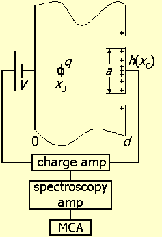
Figure 1: Semiconductor detector array with common negative contact at x = 0, and segmented positive contact at x = d, and electronic circuit of a pixel. A charge q, located at a point x0 within a square pixel of side a, induces charges on the contacts. The circuit includes charge sensitive preamplifier, spectroscopy amplifier, and a multi channel analyzer (MCA).
The charge q induces a charge distribution qw(x0, y, z) on the positive contact calculated by the method of images [3]:
 (1)
(1)
where y and z are the plane coordinates of the contact. The weight function w(x0, y, z) is the induced charge distribution on the positive contact by a unit charge within the detector.
The charge h'(x0) induced over all the positive contact is calculated directly [4, 5]:
h'(x0) = qx0/d (2)
The charge h(x0)on a single pixel is:
![]() (3)
(3)
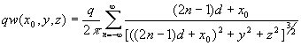
Fig-2 shows the charge h(x0), 0 < x0 < d, for a/d = 0.4, calculated by equation (3).
When the charge q moves from a position x1 to a position x2 within the detector, it will induce electric charge flow in each pixel circuit given by:
e(x1, x2) = h(x2) - h(x1) (4)
This flow is determined by the initial and final positions of the moving charge and not by the specific trajectory of the movement, and it can be calculated by applying (1), (3). Thus, the charge flow and build up in the external circuit of a pixel (4) is related to the movement of a charge within the detector bulk by applying the weight function w(x0, y, z) (1).
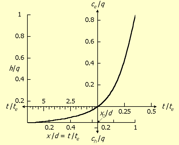
Figure 2: The charge h(x0), induced at a pixel by a charge q, located at a position x0 (equation (3)), for a/d = 0.4. The same functional dependence presents charge flow at the pixel circuit, induced by hole and electron movement within the detector. Shifting the coordinates' origin to x0 relates to gamma generation of hole-electron pairs at x0. The upward and rightward pointing coordinates relate to flow induced by electrons, and the leftward and downward pointing coordinates relate to the flow induced by the holes. The hole mobility is 10% of the electron mobility. The charge unit is the gamma generated charge q. The time unit te is the electron transition time from contact to contact.
A gamma photon absorbed at x0 generates equal amounts of holes and electrons. These charges will separate efficiently at x0 if the external electric field is stronger than their own electric fields, and move towards the opposite contacts. They move at a constant speed, v = μ iV/d, along the parallel electric field lines. μ i are the corresponding hole and electron mobility. If the pixel is not too small, transverse charge diffusion can be neglected [1]. Electrons flow from x0 toward the pixel, and holes flow away from it. Their position is given by x(t) - x0 = vt. The induced charge flow at the pixel circuit is given by (4) for x1 = x0 and x2 = x(t).
The same functional dependence of Fig. 2 presents the charge flow at the pixel circuit, induced by the hole and electron movement within the detector. Shifting the coordinates' origin to x0 relates to gamma generation of hole-electron pairs at x0.
The flow may be presented either vs. the position of the moving charges, or vs. time, since the charges move at a constant speed. It is assumed that the hole mobility is 10% of the electron mobility. The electron transition time from contact to contact te = d2/μeV is a covenient time unit.
The upward and rightward pointing coordinates of fig. 2 relate to flow induced by electrons, and the leftward and downward pointing coordinates relate to the flow induced by the holes.
Fig. 2 shows that the electrons mainly contribute to the charge build-up when they arrive near the pixel contact. The holes' contribution is distributed over a number of pixels.
The charge build-up induced over all the positive contact, q (x(t) - x0)/d, (equation (2)), is equal to the integral flow at any cross section of the detector circuit. Since all the positive contact is at the same potential, there will be also lateral charge flow between adjacent pixels, via the circuit connections. This converging radial flow, towards the arrival point of the gamma charge, is the origin of the small pixel effect.
Assume now that the holes are stationary. The holes stay at x0 and the electrons flow all the way to d. The induced charge build-up at the pixel circuit, when the electrons arrive to the pixel, is:
e(x0, d) = q - h(x0) (5)
since h(d) = q by (3).
Fig-3(a) shows the dependence of this charge on the position x0 of gamma generation. The line shape is the inverted line of fig-2.
Figure 3: (a) The charge step, e(x0, d) (equation (4)), at a pixel contact, induced by gamma charge flow from the point of photon absorption, x0, to the positive contact at d. (b) The pulse height, of a spectroscopy amplifier output, that corresponds to the input (a).
Repetition of gamma generation events many times, will yield spectral signal distribution. The distribution may be expressed in terms of the charge distribution n(e) or the absorption depth spatial distribution, n(x0).
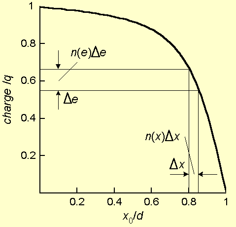
Figure 4: The number of events in the distance interval Δx is equal to the number of events in the charge interval Δe.
Fig. 4 shows that the number of events in the distance interval Δx is equal to the number of events in the charge interval Δe:
n(e)Δ(e) = n(x0)Δx0) (6)
For uniform gamma charge generation within the detector bulk,
n(x0) = 1, the charge distribution is calculated from
(5):
n(e) = (d(e(x0, d))/dx0)-1 = -(dh(x0)/dx0)-1 (7)
Since the gamma generated charge is proportional to the gamma energy, the distribution n(e) is the ordinary gamma spectrum.
Fig. 5 shows the spectra for the series: a/d = 0.2, 0.4, 0.8, 1.6, according to equation (7). The spectral lines are narrow as the aspect ratio is low and they tend towards a square shape at high ratio. The missing charge of the stationary holes generates a low energy tail in the spectrum of the small pixel detector.
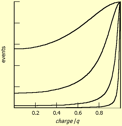
Figure 5: The charge spectral distribution, n(e) (equation (7)), for uniform gamma generation within the detector, for the series of aspect ratios: a/d = 0.2, 0.4, 0.8, 1.6.
3. Detector circuit.
The detector circuit includes a charge
sensitive preamplifier, a spectroscopy amplifier, and a multi channel analyzer
(MCA) as presented in Fig. 1.
The charge sensitive preamplifier measures the charge flow and build-up on the pixel contact, and outputs a step like signal, e(t), with rise-up that follows equation (4) and fig-2. Equation (5) gives the step's height.
The charge signal is inputted into the input of a spectroscopy amplifier that outputs a moving average of the derivative of the input. The exact output depends on the transfer function of the specific device. Here the unit will be considered a true integrator of a moving time window of a duration tshape. This operation cuts the system noise for all times except the time of charge flow through the detector.
The output is proportional to the input's finite difference, e(t) - e(t - tshape), and the pulse peaks when the electrons arrive to the pixel by eq. (5) :
S = q - h(xshape) (8)
where xshape = d - v tshape.
Consider a case where the shape time, tshape, is shorter than the electron transition time from contact to contact (te). xshape is then the position where it takes a gamma generated charge excactly tshape to arrive to the pixel.
If charge is generated at a position x0 shorter of xshape , then the flow time will be longer than tshape. However, the output peak (8) takes into account input values only in the time window tshape before arrival to the pixel. Therefore, the output signal (8) will be the same for all events where x0 < xshape.
On the other hand, for each x0 > xshape, the amplifier's output will be proportional to its input. Fig. 3(b) shows the the output of the spectroscopy amplifier vs. the position x0 of gamma generation, corresponding to the input 3(a).
Fig. 3 indicates that shape time reduction below the electron transition time leads to only small reduction of the output signal. This property is unique to the small pixel detector. In single detectors the output signal is proportional to the shape time.
4. Optimal Resolution
The gamma generated electrons, flow at a
steady speed within the detector, but induce nonlinear response of charge
build-up at the pixel contact. The build-up rate is slow as long as the
electrons are far from the contact, and it speeds up when they arrive near it
(equation (4), fig. 2). This unique property of the small pixel enables further
improvement of its spectral resolution.
Fig-6 shows the time dependent signal build-up at the pixel contact, as electrons are flowing towards it. Lines (a) and (b) show the output signal of the charge sensitive amplifier for gamma charge generation at two points, x0' and x0''. x0' is shorter than xshape and x0'' is longer than it. The figure is read either vs. the time t, or, the position x(t) of the moving electrons. The position xshape is marked on the figure.
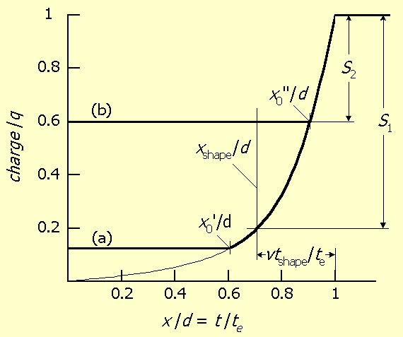
Figure 6: The signal build-up at the pixel contact, e(x0, x(t)), as electrons are flowing towards it, observed by the charge sensitive preamplifier. The figure is read vs. either the time t, or the position x(t). The position xshape is where it takes the electrons exactly tshape to arrive to the pixel. The pulse height S1, of the spectroscopy amplifier's output, is the same for all positions x0' < xshape . The height S2 is equal to the step height of the input charge for each position x0'' > xshape.
The pulse heights S of the spectroscopy amplifier, for x0' and x0'' are determined by eq. (8).
The signals of many gamma events are collected in a multi channel analyzer (MCA), and their height distribution yields the signal spectrum. For uniform gamma generation, the spectral distribution of the spectroscopy amplifier's signal will be (similarly to equation (7)):
n(S(x0) = (dS/dx0)-1 (9)
The flat part of S(x0), equation(8), fig-3(b), introduces singularity to equation (9), so that the spectrum includes a δ function. A fraction xshape/d of all the events of gamma generation, have the same value and appear as a single line. The rest of the events appear as a tail of lower values.
The single line response in the detector spectrum is broadened by the noise in the system. The main sources of noise are the detector's leakage current and the preamplifier's electronics noise.
In summary, the shape time of a spectroscopy amplifier is adjusted below the electron's transition time through a detector, to the fast signal build-up at the pixel contact. The reduced time somewhat decreases the amplifier's signal height, but also introduces a δ function contribution to its spectral response. The spectral line is broadened by the noise in the system.
The electrons flow within a single pixel, and induce fast charge build-up at its contact when they arrive near it. This unique property allows shape time reduction and adjustment to the build-up with little loss of signal height.
Fig-6 shows the calculated spectra of a single pixel detector, with xshape/d = 0.5, for the series a/d = 0.2, 0.4, 0.8, 1.6 (equation (9)). The line for a/d = 0.2 is arbitrarily noise broadened to 1%, then the noise is doubled for each consecutive line. The figure corresponds to an array where the noise is proportional to the square root of the pixel's area.
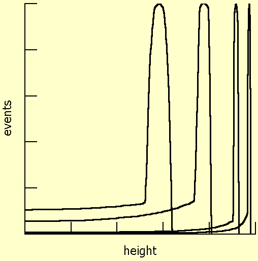
Figure 7: The pulse height spectrum of the spectroscopy amplifier's output (equation (9)), for uniform gamma generation within the detector, for the series: a/d = 0.2, 0.4, 0.8, 1.6. tshape/te = 0.5 (therefore xshape/d = 0.5). The line widths are adjusted to 1, 2, 4, 8% respectively, corresponding to noise level proportional to the square root of the pixel's area. Reduction of tshape below te, the electron transition time from contact to contact, leads to improvement of the spectral resolution, as compared to fig. 5.
The figure shows significant spectral improvement, compared to fig. 5 where the shape time is equal to the electron's transition time (and therefore, xshape = 0). Good resolution is observed for higher aspect ratio of pixel side to detector thickness, so the "small" pixel needs not be really small.
5. In practice
Bias voltage and shape time adjustment optimizes the
detector circuit operation, so that the single pixel resolution approaches the
noise limit with little loss of signal. The voltage is adjusted high enough to
avoid electron trapping, by reducing the electron's transition time through the
detector below its lifetime. The shape time is then adjusted to the fast signal
build-up period at the pixel's contact.
The optimal shape time is significantly shorter than the electron transition time, as observed in fig-3(b). In some systems the test equipment limits the short shape time value, or, the value is fixed in an integrated circuit. However, the same ratio of short shape time to the longer transition time is achieved by slowing down the electrons' flow by lower bias voltage. The resolution improves in spite of some electron trapping, as observed by Shor et al. in [6] fig. 1.
6. Conclusion
The shape time is adjusted to the fast build-up of
induced charge, at a pixel contact, and improves the energy resolution of the
detector circuit towards the noise limit. The small pixel acts as a spatial and
temporal filter with proper parameters' adjustment.
The arguments presented in this paper are valid also for a single detector. The difference is that reduction of the shape time, below the charge transition time through the detector, reduces also the output signal. Such adjustment is justified in a single detector with very low noise level.
References
on the net: 17, March 2000. Revised June 2001.
See poster, presented at the IEEE Nuclear Science Symposium, Lyon France, October 15 - 20, 2000.
by the author:
Links: