(see Improving CdTe and CdZnTe Crystals by Agitation during the Crystal Growth)
Abstract
CdTe and CdZnTe semiconductor gamma detectors equipped with ohmic contacts
are fast response devices that are not sensitive to hole trapping [1-3]. A model
of an ohmic contact is presented in effort to clarify the mechanism of their
operation.
1. Ohmic contact
Consider a conductor equipped with two parallel plate contacts of unit area
located at 0 and d as presented in figure 1. The conductor is divided at
x into two parts of different conductivity. It is assumed, for the
convenience of presentation, that the charge carriers are electrons with the
same mobility μ at the two parts. So they differ only
by the charge carrier density n1 and n2
(n1 > n2).
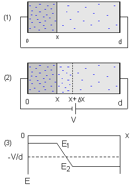
Figure 1: Conductor of two parts of different conductivity, (1) at zero bias, (2) under bias V. (3) The electric field distribution within the conductor, immediately after voltage application (dashed line), and at a steady state (continuous line).
Assume now that the electrons are free to cross the boundary between the conductors and move from side to side.
Each conductor is electrically neutral since positive stationary charge balances the negative electron charge. A charged layer may be formed at the boundary at zero bias, but it is assumed not to affect charge flow.
By application of voltage V to the contacts, with the left contact
negatively biased, all the electrons will start to move rightward at the same
speed:
so that during a time Δt they will move a distance
Δx = vΔt.
During this time n1Δx
electrons cross the boundary at x, and n2Δ x
electrons leave the volume between x and
x + Δx, leaving behind them the same
amount of positive charge. Therefore, the volume will accumulate the charge:
This space charge decreases the electric field E1 left to x and increases the field E2 right to x + Δx. So charge carriers at the left move slower than before, and therefore, enter the space charge region at a slower rate. At the right they leave it faster and move to the right faster than before.
As electrons continue to flow the thickness and charge of the layer build up
until the system reaches steady state when the two rates become equal (figure
1):
The carrier density changes continuously from n1 to
n2 within the space charge region according to Poisson
equation. The charge q accumulated in the region is given by Gauss law
(CGS units):
where the resistivity is 1/ρ = μen, and the resistance is R1 = ρ1x, R2 =ρ2(d - x), and R = R1 +R2.
Left to the boundary the electrons are dense and slow since the electric field is weak. When they cross the boundary to the right they accelerate and move fast, in proportion to the stronger electric field at the right. Consequently, the distance between neighbor electrons increases. The space charge region takes care that the same electron rate will cross any cross section in the circuit.
When the bias voltage changes, electrons flow into the space charge layer and out of it. The layer adjusts itself by changing the charge q in proportion to the voltage, in order that the same steady state carrier current will flow on its both sides. Since the net charge density is bound by n1 - n2, change of q must involve change of the layer thickness.
Assume now that ρ1 << ρ2,
call the left conductor contact
and the right conductor bulk, and here is the ohmic
contact. If the contact is much thinner than the bulk then equation (4)
will be the ordinary expression for a charge on a parallel plate capacitor:
In conclusion of these arguments, nothing blocks the entrance of electrons from the contact into the bulk. It is all a matter of electron speed control by the space charge layer. This layer adjusts the electric fields in the contact and in the bulk in a way that the slow flow of many electrons in the contact will be exactly equal to the fast flow of few electrons in the bulk.
There are no standing electrons within the space charge layer at the border
between the contact and the bulk. All the electrons are moving. The charged
layer is formed by a small shift of the dense electron charge of the contact
into the bulk. This charge is the source or sink of the electric field lines
within the bulk as is required by Poisson equation.
2. Photoconduction
Light generates electron hole pairs in a photoconductor and they disappear by charge recombination. The balance between the two processes determines the density of charge carriers, which in turn, determines the bulk resistance. The ohmic contact operates in this system as described in the previous section. However, the contact and the space charge layer respond to density changes of the photo carriers instead of responding to a changing voltage.
Figure 2 shows the Fermi level and energy band diagram of an ohmic metal
contact to a semiconductor bulk. The resistance of the metal contact is far
below the bulk resistance. However, it is considered finite, while all the other
resistance in the circuit is assumed zero. So, the sum of the voltages on the
contact and on the bulk is equal to the constant bias voltage, V =
Vcontact + Vbulk. The bias voltage is divided by the corresponding
contact and bulk resistance, so that almost all of it falls on the bulk.
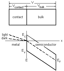
Figure 2: The Fermi level and energy band diagram of an ohmic metal contact
to a semiconductor bulk. The metal and semiconductor energies are plotted on
different scales. Light illumination increases the slope of the Fermi level
within the metal compared to the dark.
The tilt of the energy bands in figure 2 presents the electric field within the materials. The field within the contact is much smaller than the field within the bulk, therefore, they are presented on different scales in the figure.
Electrons flow within the metal contact, but only those with energy above the edge of the conduction band can flow into the semiconductor. When the bulk is illuminated by light its resistance decreases, and therefore, the bias voltage will be redistributed between the contact and the bulk. The effect on the bulk voltage is negligible, but the contact voltage will change significantly and will linearly increase with the light level. This change is presented in the figure by the Fermi level slope within the metal contact. Illumination increases the slope compared to the slope in the dark.
The number of electrons in the metal contact, with energy above the edge of the conduction band, does not change by light illumination. However, forced by the higher contact voltage, they will move at a faster speed that is linear with the light level. Therefore, the number of electrons that enter the bulk will also be linear with the light level.
These arguments lead to important practical conclusion. If the contact is ohmic with respect to the dark current, then it will be ohmic also with respect to the photocurrent. The contact is able to supply photocurrents, that are many orders of magnitude higher than the dark current, because the electrons in it move faster by the corresponding higher contact voltage. This conclusion is clearly limited to single carrier conduction. The case of two carrier conduction, electrons and holes, requires separate and more detailed discussion.
Whenever charge carriers leave the bulk via one contact, similar carriers will enter it via the other contact. Charge disappears from the system by electron hole recombination. If the light is turned off the photocurrent will not stop but continue to flow and decay as electrons and holes disappear by recombination. The lifetime of the photo generated charge may become very long at low temperatures and the currents may last days. Such currents are persistent currents.
Another effect is observed in semiconductors. Charge is trapped in levels
that are distributed within the forbidden band, and the recombination cross
section varies appreciably between different levels. After the light is turned
off the current will decay by charge recombination. Initial fast decay proceeds
via traps or recombination centers of large cross section. However, charges in
traps of small cross section, contribute to residual after-glow current that may
continue to flow for hours.
3. Gamma detection
A gamma photon, that is absorbed in a semiconductor, generates a number of
electron hole pairs that is proportional to its energy. Typically, about 4 eV is
required to generate a pair, so a 100 kev photon will generate about 25000
pairs. This charge measures the photon energy.
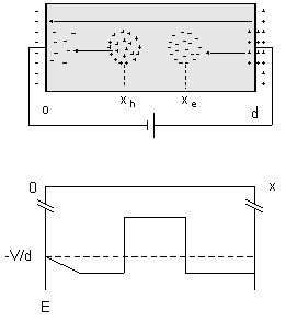
Figure 3: Flow of gamma generated charge within a detector. The electric field at the negative contact is unchanged and electrons enter the bulk from it, flow towards the holes and recombine with them. Three representative electric field lines are shown.
The gamma generated charge is a source or sink of electric field lines that
induce charge on the contacts. However, the external bias voltage produces
electric field that is much stronger than the field induced by the gamma charge,
in order to overcome the attraction between the positive and negative gamma
generated charges. Therefore, all the field lines become nearly parallel to each
other and perpendicular to the contacts (figure 3), and the gamma induced charge
flows along them. The one dimension geometry allows calculation of the electric
field by application of Gauss law. A charge q located at x between
the contacts will change the electric field on its left and right sides by the
amounts:
The overall electric current involved with the flow of q is the sum of
carrier and displacement currents:
The current is calculated, by using equations (6) - (7), as a displacement
current at any cross section where there is no carrier flow:
This calculation holds for any extra charge that flows between the contacts.
Therefore, by (1), the current of the gamma generated holes and electrons will
be:
where q is the gamma generated charge.
Since the overall current is the same at any cross section of the circuit, the current (9) is equal to the charge carrier current at any place in the electrical wires and contacts. Therefore, it is also equal to the rate that electrons enter into the bulk from the negative contact.
As discussed in section 1, the electrons that enter the bulk, accelerate to a
higher speed, and become negative space charge Δq. This negative charge reduces the electric field at
its left side on the contact, according to equation (6):
where Δx is the charge penetration depth. This reduction should have slowed down the electrons that follow up in the contact had it been the only change. However, the separated gamma generated charges decrease the field between them and increase it outwards. So they increase it also at the contact:
where xh and xe are the positions of the gamma generated holes and electrons.
The combined effect of all the charge induced fields, outlined in figure 3,
leaves the electric field unchanged at the contact. Therefore, the electrons
that come out of it continue to flow into the bulk towards the holes and
recombine with them. The two equations (10)-(11) relate the various charges and
their positions:
Since the electrons are about ten times faster than the holes, the holes travel only a short distance during this period. There will be only small difference if they are trapped and do not move at all. In any case, the time required to hole flow, all the way to the negative contact, is saved. This process is an automatic mechanism of hole detrapping.
Reference [1] gives calculation of the collection time that is based on
equation (12). In summary, a detector equipped with ohmic contacts is a fast
response device that is not sensitive to hole trapping.
4. Contact realization
Ohmic contact fabrication to various materials is a challenge. The contacts
in gamma detectors should be ohmic with respect to both the dark leakage current
and the gamma induced current. Contact fabrication to n-type material is easier
since both currents are electron currents, in contrast to p-type material where
the leakage is a hole current. The contact performance may also depend on the
voltage polarity, and different materials may be required to negative or
positive bias. Some details are in the references [1] - [3].
5. Conclusion
The ohmic contact operation involves space charge, as discussed above in the
three systems. The flow of gamma generated charge in detectors equipped with
ohmic contacts induces additional charge flow from the contacts into the bulk.
Electrons, that come out of the negative contact, flow towards the holes and
recombine with them. This flow shortens the gamma charge collection time and
overcomes hole trapping. The effect of the ohmic contact stems from fundamental
principles based on the continuity and Poisson equations.
Comments welcomed: urila@internet-zahav.net
on the net: 24, July 1998. revised: 24, September 1998
by the author:
Links: