(see revision, February 2000).
Abstract
Semiconductor gamma radiation detectors equipped with ohmic
contacts are fast response devices that are not sensitive to hole
trapping. Ohmic detector arrays can be fabricated from crystals of CdTe or CdZnTe that grow by standard techniques.
1. Introduction
CdTe and CdZnTe semiconductor crystals are used for room temperature gamma radiation detection. Chlorine doped CdTe grows by the traveling heater method (THM), that yields high quality single detectors, but the crystal is not uniform and the detectors are small. A growth rate of few millimeters per day is slow, and the crystal size is limited.
In high pressure Bridgman (HPB) growth of CdZnTe the crystal size is not limited, and a growth rate of few millimeters per hour is fast. The higher band-gap CdZnTe yields material of higher electrical resistivity, and therefore, larger size detectors become available. However, crystal uniformity is still a problem, and sometimes, also hole trapping. Handling the high pressure system is inconvenient.
CdTe and CdZnTe grow by standard Bridgman techniques for substrate production. However, they do not yield detector grade material.
Hole and electron charges, generated by a gamma photon in a semiconductor detector, flow in opposite directions towards the contacts. It has been proposed [1, 2] that if the contacts are ohmic then additional charge will flow from the contacts towards the gamma generated charge. The ohmic contact effect transforms the detector into a fast response device that is not sensitive to hole trapping.
Detector operation is characterized by its leakage current and the μ τ (mobility times lifetime) values of both the holes and electrons. The lifetimes depend on the traps density and distribution within the forbidden band. Levels that lie above the Fermi level act as electron traps, and levels below it act as hole traps. In a case of mid gap levels, shift of the Fermi level, upward or downward, will increase the lifetime of one carrier on expense of the other carrier.
In conventional detectors full collection of the gamma generated holes and electrons is required in order to have good energy resolution. Trapping of either carrier will degrade the detector performance. The total trap density should be low so that both lifetimes will be long enough to allow full charge collection.
Ohmic contact detectors are not sensitive to hole trapping, hence, the holes lifetime can be shortened and the electrons lifetime can be increased by pushing up the Fermi level. In this way electron trap levels go below the Fermi level and become inactive. The conductivity increases from its p-type minimum to an n-type value of optimal combination of leakage current and electron lifetime.
The possibility to improve the ohmic detector performance, by increasing its conductance, enables preparation of good quality detectors from material that initially has too many traps. Therefore, standard crystal growth techniques, used for substrates, can be considered for production of ohmic detectors and detector arrays.
Since the operation of the ohmic detector depends mainly
on the electrons, and not on both the electrons and holes, ohmic
arrays are expected to be more uniform than conventional arrays.
2. crystal growth
CdTe crystals grow by the Bridgman technique in a closed ampoule with small tellurium excess. Therefore the pressure in the ampoule is nearly equal to the tellurium vapor pressure at the growth temperature. Under these conditions the crystal contains excess of tellurium atoms that during cool down come out as precipitates, mainly at dislocations and grain boundaries.
The crystal quality improves by applying the modified Bridgman technique[3 - 6] where one ampoule end is kept at lower temperature. There is a small cadmium excess in the ampoule. So the cold end determines the cadmium vapor pressure that is nearly equal to the over all pressure.
Fig. 1 and fig. 2 present the horizontal and vertical versions
of this process. In both cases the crystal grows from the melt
by moving it along a region with temperature gradient that extends
from above to below the melting point. The cold end temperature
determines the cadmium vapor pressure, that remains constant during
the growth process.

Fig. 1: Crystal growth by horizontal modified Bridgman
The growth may proceed by mechanically moving the ampoule,
or, by moving the heating furnace. In recent systems the furnace
is built of many heating zones and a computer controls the temperature
profile. The computer shifts the profile electronically and there
are no mechanically moving parts within the furnace [4 - 6].
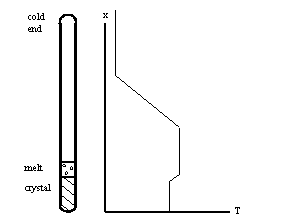
Fig. 2: Crystal growth by vertical modified Bridgman
The growth procedure starts by melting the separate cadmium
and tellurium loads, under hydrogen atmosphere, in order to remove
oxygen from the system [5 - 6]. The materials are then brought
into contact and heated until they react and produce CdTe, or,
CdZnTe if zinc is also present. Good quality crystals, practically
free of precipitates, grow when the cold end temperature is about
300o C below the melting point, and when this difference
stays during the cool down stage [3, 5]. Further details of the
crystal growth process are also in the literature.
3. Control of the electrical conductivity
High resistivity pure CdTe is not a good gamma detector since the lifetimes of the gamma generated holes and electrons are relatively short. Addition of dopants, mainly chlorine or indium [7], activates the material. The amount of chlorine that may be introduced into the crystal is limited, but there is no such limit with indium. These dopants act as electron donors in CdTe so that the crystal is expected to become highly conducting n-type. However, tellurium excess in the crystal transforms the dopants into a compensated state resulting in a crystal of high electrical resistivity and high sensitivity to gamma radiation.
In crystals that grow by modified Bridgman the amounts of cadmium and tellurium are balanced, therefore, addition of donor dopants will make them highly conducting. However, by annealing the crystal in saturated tellurium vapors, tellurium atoms will diffuse into it, or, cadmium atoms will diffuse out of it, and transform the dopants into a compensated state. Annealing at low enough temperature will not damage the crystal and precipitates will not appear.
Diffusion processes are slow at low temperatures. Cutting the crystal into wafers of the required thickness, before this step, will reduce the annealing time [8]. One end of the annealing ampoule should be kept at somewhat lower temperature in order to avoid tellurium vapor condensation on the wafers when it cools down [8].
The residual uncompensated donors determine the degree of electrical conductivity. The amount of donors is a fraction of the over all dopant amount, and increase of the over all doping will increase the donor amount as well. Therefore, the electrical conductivity will also increase. The conductivity is, therefore, controllable by adjustment of the doping level.
Donor dopants have two-fold effect within the crystal. In a compensated state they neutralize traps, and in an uncompensated state they push up the Fermi level and inactivate electron trap levels that go below it. Therefore, higher doping level will increase the electron lifetime, but it will also increase the leakage current and the current noise. A series of iterations of crystal growth experiments with different doping levels, followed by subsequent annealing, can yield optimal detector composition.
In summary, doped crystals come out highly conducting under
optimal crystal growth conditions. Annealing in tellurium vapors
can transform them into a compensated state of high electrical
resistivity and high sensitivity to gamma radiation. The electrical
conductivity, in this state, is controllable by adjustment of
the doping level.
4. Device fabrication
Device fabrication can proceed by standard techniques. Mechanical polishing removes the cutting damage from the wafers, then they are chemically etched by a solution of bromine in methyl alcohol. Recently solutions of bromine in ethylene glycol have become popular [9].
Chemical deposition of gold or platinum does not yield good
ohmic contacts to n-type material. Contacts to semiconductors
are usually prepared by deposition of thin metal film followed
by heat treatment. Advanced designs apply multi layers of different
metals and other materials. Evaporated indium or aluminum can
be used as ohmic contacts to n-type CdTe or CdZnTe. Indium, however, cannot be heated above its low temperature melting point, 156o C, and a double layer of indium and aluminum may enable heat treatment at higher temperatures. There is a need, however, of further development of ohmic contacts to CdTe.
5. References
On the net: 22, March 1998
by the author:
Links: